
 Newsletters




Huawei announced Monday it has developed a new engineering approach called "LogicFolding" to produce next-generation smartphone chips, as the Chinese technology company faces continued U.S. export restrictions and increasing competition from Nvidia and Apple in global markets.
Huawei said the new method will be used in Kirin processors coming out this fall. The company claims that by moving the chip layout from a single to a dual-layer architecture, the architecture allows transistors to connect at more points, making the chips more energy efficient.
According to Huawei, this technology could match the capabilities of a 1.4-nanometer production process by 2031.
Global chipmaking leader TSMC has already begun mass production of 2-nanometer chips. Smaller nanometer-scale nodes generally enable faster, more power-efficient semiconductors.
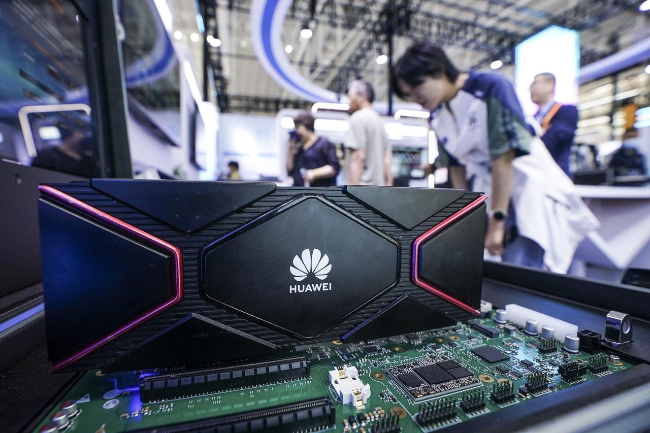

Some analysts are skeptical. Paul Triolo, who leads the technology unit at DGA Group, said this approach is more about system-level optimization, such as "shortening wires, stacking logic layers, improving memory semantics and co-designing chips, packaging, software and clusters," rather than a real breakthrough in chip-making processes. He also pointed out that there are still big challenges with heat management and large-scale production.
Neil Shah, research vice president at Counterpoint Research, said Huawei's alternative approach to semiconductor manufacturing has not yet been proven at scale.
He warned that it could bring new problems with heat and packaging, potentially lowering manufacturing yields.
NVIDIA Chief Executive Jensen Huang told CNBC last week that the U.S. chipmaker has effectively "ceded" the Chinese market to Huawei.
George Chen, co-chair and partner at The Asia Group, said the development signals a narrowing window for Nvidia to sell advanced chips such as the H200 in China and is likely to deepen concerns in Washington, where Huawei remains a symbol of U.S. export control policy.
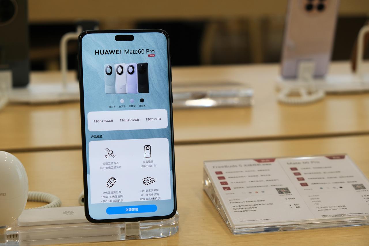
Huawei's Mate 60 smartphone, released in 2023 with 5G and an advanced chip, helped the company win back market share from Apple in China.
Huawei has been blocked from accessing advanced extreme ultraviolet (EUV) lithography machines made by Dutch equipment manufacturer ASML, pushing the company to pursue alternative chip development pathways.
Along with the chip announcement, Huawei said it wants more academic recognition for its semiconductor research. The company called its findings the "Tau Law" or "τ scaling" and presented it as a way to address industry challenges.
Huawei said it has developed 381 chips using the τ scaling framework over the past six years, and all of them have entered mass production.
This announcement comes as the semiconductor industry is moving away from Moore's Law, which states that the number of transistors on a chip doubles approximately every 2 years. NVIDIA CEO Jensen Huang has also said this rule no longer fits future chip development.
Tingbo He, who leads Huawei's semiconductor unit, admitted that the company is just beginning a development process that could take 10 years and that there are still major challenges ahead.
Shah said that using this technology in the upcoming Mate 90 series would be a big engineering achievement. However, the real test for China's way around Western sanctions will be whether it can be scaled up for artificial intelligence data centers.


 Set as preferred source
 Set as preferred source



 2 min read